At first glance, USB 3.x does not appear dramatically different from USB 2.0. The connectors look familiar. The cables often look similar. A USB flash drive still plugs into a computer the same way it has for years.
Because of this, many people assume USB 3.x is simply a faster version of USB 2.0. USB 2.0 transfers data at 480 Mbps, while USB 3.0 increases that speed to 5 Gbps. On paper, that sounds like a straightforward improvement.
The reality is much different.
USB 3.x does not merely move data faster. It pushes electronic signals into a range where engineering challenges increase dramatically. Effects that were once insignificant suddenly become important. Components that were once simple become precision parts. Design decisions that barely mattered at USB 2.0 speeds can determine whether a USB 3.x product works reliably or fails intermittently.
One way to understand the difference is to think about automobiles.
A family sedan can comfortably travel at 65 miles per hour. Small imperfections in tire balance, suspension alignment, road surface, or aerodynamics may never be noticed by the driver. The vehicle remains stable and predictable.
Now imagine asking that same car to travel at 300 miles per hour.
Suddenly everything changes. Tire balance becomes critical. Aerodynamics become critical. Suspension geometry becomes critical. Tiny imperfections that were irrelevant at highway speeds can become dangerous at racing speeds.
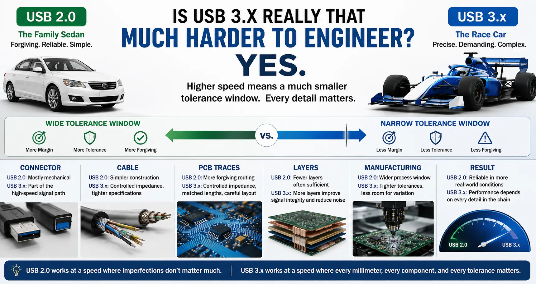
USB 2.0 is the family sedan. USB 3.x is the Formula One race car.
The challenge is not simply going faster. The challenge is maintaining control while operating at speeds where every detail matters.
USB 3.x Moves Into a Different Engineering World
This principle surprises many people because USB technology is often viewed as a digital system. Data is either a one or a zero. A device either works or it does not.
At USB 2.0 speeds, that viewpoint is often good enough.
At USB 3.x speeds, engineers begin entering a world that looks much closer to radio frequency engineering. Signals no longer behave like simple on-and-off switches. They behave like high-frequency waveforms traveling through a complex physical path.
This changes how engineers must think about the entire design.
A USB connector is no longer just a connector.
A cable is no longer just a cable.
A printed circuit board trace is no longer just a piece of copper.
Every part of the signal path becomes part of the communication system.
A signal leaving the USB controller travels through circuit board traces, solder joints, connectors, cables, additional connectors, and more circuit board traces before reaching its destination. At USB 2.0 speeds, many imperfections along this path can be tolerated. At USB 3.x speeds, those imperfections can create reflections, signal loss, timing variation, and communication errors.
The Tolerance Window Gets Much Smaller
The easiest way to visualize this is to think in terms of engineering margin. USB 2.0 has a much wider tolerance window. USB 3.x has a much narrower one. The product may look the same from the outside, but internally the room for error is dramatically smaller.
USB 2.0 vs USB 3.x: Engineering Tolerance Comparison
Click to expand engineering comparison chart
| Design Area | USB 2.0 | USB 3.x | Why It Matters |
|---|---|---|---|
| Signal Speed | 480 Mbps | 5 Gbps, 10 Gbps, or higher | Small physical imperfections become electrically significant. |
| Connector Role | Mostly a mechanical connection | Part of the high-speed signal path | Contact quality, geometry, and wear can affect reliability. |
| PCB Traces | More forgiving routing | Controlled impedance and careful routing | Trace shape, length, and spacing influence signal quality. |
| Manufacturing Margin | Wider tolerance window | Narrower tolerance window | Small variations can cause intermittent failures. |
| Debugging Difficulty | Usually easier to isolate | Often system-level and intermittent | The problem may come from the interaction of several marginal parts. |
Why USB Flash Drives Become Harder
This challenge is especially clear in USB flash drive development.
Many consumers assume a USB flash drive is a simple product. Externally, that assumption seems reasonable. A flash drive is small, lightweight, and visually uncomplicated.
Internally, however, a USB 3.x flash drive requires significantly more engineering discipline than its USB 2.0 counterpart.
The routing of high-speed differential signal pairsThe precise design and layout of paired signal traces that carry high-speed differential signals to ensure signal integrity and performance. must be carefully controlled. Trace lengths may need to be matched. Signal impedance must remain within strict limits. Return current paths must be considered. Crosstalk between nearby signals must be minimized. Even routing decisions measured in millimeters can influence performance.
The small physical size of a flash drive does not remove the challenge. In many cases, it increases the challenge because engineers must fit high-speed circuitry into a very compact space while still maintaining signal integrityThe quality and reliability of electrical signals as they travel through a communication system..
Why More PCB Layers May Be Needed
The same trend appears in printed circuit board design.
When people hear that a product uses a twelve-layer or sixteen-layer circuit board, they often assume the additional layers were added to support more features. Sometimes that is true, but high-speed digital design introduces another reason.
Additional layers give engineers better control over signal behavior.
Dedicated ground planes improve return current paths. Carefully controlled layer structures help maintain impedance targets. Additional routing layers can reduce crosstalk and electrical noise. The extra layers are not always about adding functionality. Often they are about improving predictability.
At USB 2.0 speeds, a designer can often route signals around obstacles and still produce a reliable product. At USB 3.x speeds, the designer may need to build the board around signal integrity requirements from the beginning.
This is similar to what is happening in advanced semiconductor design, where engineers are looking beyond simple scaling and toward three-dimensional structures to improve performance, density, and signal paths. The same general idea appears in newer chip research, such as 3D silicon circuits moving closer to reality.
Manufacturing Becomes Less Forgiving
Manufacturing introduces another layer of complexity.
A USB 2.0 design may continue functioning properly despite modest variations in materials, assembly processes, or component quality. USB 3.x systems generally operate with smaller performance margins. Connector consistency becomes more important. PCB fabrication tolerances become more important. Solder quality becomes more important. Assembly precision becomes more important.
The product may look identical to the customer, yet require significantly tighter manufacturing controls behind the scenes.
This is one reason engineers sometimes encounter situations where a USB 2.0 connection appears perfectly reliable while a USB 3.x connection experiences intermittent errors, retries, resets, or reduced performance.
Nothing may actually be broken.
Instead, the system has reached a point where imperfections that were once insignificant have become relevant.
The race car is now traveling at racing speed.
USB 3.x Is More Than a Speed Increase
A useful way to think about USB 3.x is that it represents more than a speed increase. It represents a shift into a different class of engineering problem.
The transition from USB 2.0 to USB 3.x requires engineers to think differently about connectors, cables, circuit boards, manufacturing tolerances, signal integrity, and system interactions. The challenge extends far beyond moving more bits per second.
For consumers, the difference may be measured in faster file transfers.
For engineers, the difference is often measured in additional testing, more sophisticated designs, tighter manufacturing controls, and a much deeper understanding of how high-speed electronic signals behave in the real world.
So is USB 3.x really that much harder to engineer?
Yes.
Not because it is simply faster, but because it operates in a realm where details that once seemed insignificant suddenly become essential.
Editorial Note: This article is based on publicly documented USB specifications, high-speed digital design principles, PCB design practices, signal integrity concepts, and real-world observations from USB hardware development and testing. While examples and analogies are simplified for educational purposes, the underlying engineering concepts reflect challenges commonly encountered when designing and manufacturing high-speed USB 3.x products.
Let GetUSB.info keep you updated.
Receive article notifications about USB storage, flash memory, and duplication updates in your preferred language. We average a couple of articles per week.