AI infrastructure has a way of exposing limits that most systems never run into.
In the earlier pieces, we looked at how high bandwidth memory for AI workloads keeps data as close to the GPU as possible, and how storage class memory between DRAM and NAND helps smooth out the gap between active memory and traditional flash storage. Both of those layers exist because the system can’t afford to wait, even for short periods of time, without losing efficiency.
But there’s another direction the industry is moving in, and it doesn’t involve introducing an entirely new type of memory.
Instead, it’s taking something that already exists, NAND flash, and pushing it into a role it wasn’t originally designed for.
That’s where the idea of High Bandwidth Flash starts to come into the conversation.
The Problem NAND Was Never Meant to Solve
NAND flashA type of non-volatile storage technology designed to store large amounts of data efficiently and retrieve it when needed. has always been built around a simple idea: store a lot of data efficiently and retrieve it when needed.
For most workloads, that model works perfectly well. Data sits on storage, the system requests it, and the SSD delivers it fast enough that nobody really notices the delay.
AI workloads change that dynamic.
Instead of occasional reads and writes, these systems are constantly pulling data in parallel, often across thousands of threads, with very little tolerance for inconsistency in delivery. It’s not just about speed in isolation, it’s about maintaining a steady flow of data that keeps the compute side fully utilized.
That’s where traditional NAND behavior starts to show its limits.
Even high-performance NVMe drives, with deep queues and strong throughput numbers, are still operating within a storage model that assumes bursts of activity, not a continuous, memory-like stream of access.
So the question becomes: what happens if you stop treating NAND like storage, and start treating it more like part of the memory system?
What “High Bandwidth Flash” Actually Means
High Bandwidth Flash isn’t a formal standard or a single product category.
It’s better understood as an architectural direction, and that’s where it starts to separate itself from what we covered in High Bandwidth Memory.
High Bandwidth Memory is still memory. It’s DRAM, built and positioned to deliver extremely fast access by sitting physically close to the processor. The entire point of HBM is proximity and latency reduction, getting data as close to compute as possible so it can be accessed almost instantly.
High Bandwidth Flash is solving a different problem. It accepts that NAND sits further away in the system and carries higher latency, and instead focuses on how to move much larger amounts of data in parallel so that distance matters less.
In simple terms, HBM is about making memory faster by bringing it closer. High Bandwidth Flash is about making storage behave faster by changing how it’s accessed.
That distinction matters, because the goal here isn’t to turn NAND into DRAM. It’s to make NAND useful in situations where traditional storage would otherwise slow the system down.
The shift happens at the system level, not just at the media level.
Instead of a single SSD servicing requests in a traditional way, you start to see many NAND channels operating in parallel, controllers designed for concurrency rather than just capacity, wider data paths through PCIe Gen5 and Gen6 interfaces, and software layers that anticipate and stage data before it’s requested.
Taken together, these changes don’t eliminate NAND’s inherent latency, but they reduce how often that latency becomes the limiting factor in the system.
A Different Way to Think About Bandwidth
When people hear “high bandwidth,” the assumption is usually raw speed.
But in this context, bandwidth is really about how much data can be moved at once, and how consistently that movement can be maintained.
AI workloads don’t just need fast access, they need predictable access at scale.
If a GPU clusterA group of interconnected GPUs working together to perform parallel processing tasks. is pulling data unevenly, even small variations can cause parts of the system to stall. Multiply that across hundreds or thousands of nodes, and those inefficiencies start to show up in ways that are difficult to ignore.
High Bandwidth Flash is an attempt to smooth that out, not by eliminating NAND’s characteristics, but by surrounding it with enough parallelism and intelligence that those characteristics matter less to the overall system.
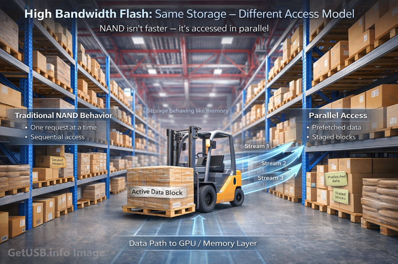
Extending the Warehouse Analogy
If we keep using the same warehouse model from the earlier articles, NAND has always been the main storage floor.
It’s where everything lives, organized in rows and shelves, optimized for density and efficiency rather than speed of access.
DRAM is the loading dock, where active work happens. SCM is the staging area just behind it.
High Bandwidth FlashAn architectural approach to optimize NAND flash storage for parallel data access, improving throughput and consistency for demanding workloads. changes how the warehouse operates.
Instead of a single worker walking into the aisles to pick items one at a time, you now have multiple loading docks open at once, with several forklifts moving in parallel, and items being pre-staged based on what the system expects to need next.
The warehouse hasn’t changed fundamentally, but the way it’s being accessed has.
You’re not turning the warehouse into the loading dock, you’re making the warehouse behave like it’s much closer to it.
How This Is Being Built in Practice
Most of what enables High Bandwidth Flash doesn’t come from the NAND itself, but from the layers around it.
Controllers now play a larger role in how data is distributed, focusing on parallel operations across multiple NAND dies and channels instead of simply managing capacity and wear. At the same time, interface bandwidth continues to expand, giving these systems more room to move data without becoming constrained by the bus.
What makes the biggest difference, though, is how the software interacts with the hardware.
Data is no longer just fetched when requested. It’s predicted, staged, cached, and organized in ways that align with how AI workloads behave. That means anticipating access patterns, keeping frequently used data closer to the top of the stack, and minimizing how often the system has to fall back to slower paths.
None of this turns NAND into true memory, but it allows it to participate in the memory system more actively than before.
What It Still Is Not
For all of this progress, it’s important to keep expectations grounded.
High Bandwidth Flash does not make NAND equivalent to DRAM. It is still block-based, still carries higher latency than any form of true memory, and still depends heavily on controllers and software to perform well in demanding environments.
Those constraints don’t disappear, they’re simply managed more effectively through system design.
Where This Fits in AI Infrastructure
In real-world deployments, High Bandwidth Flash is showing up in systems that need to handle extremely large datasets without pushing everything into expensive memory tiers.
What this really looks like in practice is a system that leans on NAND more actively than it used to, not just as a place where data is stored, but as part of the working data path that feeds compute resources in a more continuous way.
In large-scale inference environments, for example, models and context data often exceed what can realistically fit inside DRAM. Instead of forcing everything into memory, the system relies on high-throughput access to NAND, allowing data to stream in fast enough that it behaves more like an extension of memory than traditional storage.
In training environments, where datasets are constantly being revisited and processed in parallel, the goal shifts toward maintaining a steady flow rather than handling isolated bursts. High Bandwidth Flash supports that by keeping multiple data paths active at once, reducing the chances that any single request becomes a bottleneck.
Even in distributed NVMe fabric systems, the idea remains the same. Data is spread across many devices and nodes, but accessed in a coordinated way that emphasizes throughput and availability over simple storage capacity. NAND is still doing the same fundamental job, but the way the system interacts with it is far more dynamic than it used to be.
The end result is that NAND stops behaving like a distant layer at the bottom of the stack and starts to feel like it’s part of the active system, even if it never fully reaches the performance characteristics of memory.
Why This Direction Matters
If you step back and look at what’s happening across all three of these articles, a pattern starts to emerge.
HBM moves memory closer to compute. SCM reduces the gap between memory and storage. High Bandwidth Flash pushes storage closer to memory.
Everything is converging toward the same goal: reducing how far data has to travel, and how long the system has to wait for it.
Bringing It Back to the Bigger Picture
NAND isn’t going away.
If anything, it’s becoming more important, because the total amount of data these systems need continues to grow.
What’s changing is how NAND is being used.
It’s no longer just a passive layer at the bottom of the stack. It’s being pulled upward, integrated more tightly, and asked to behave in ways that look increasingly like memory, even if it never fully becomes it.
That shift is exactly what we pointed to in the original piece: the industry didn’t replace NAND, it built around it.
What Comes Next
From here, the stack continues to evolve in both directions.
Above, memory becomes faster and more specialized. Below, storage becomes more intelligent and more integrated. And somewhere in the middle, the line between the two keeps getting harder to define.
In the next piece, we’ll look at how AI systems handle working data in real time, and why concepts like context and KV cache are starting to influence how memory and storage are designed together.
Editorial Note
This article’s perspective, direction, and technical framing were guided by the author, based on the specific themes explored throughout the piece and the broader discussion around how NAND is being pushed closer to the memory layer in AI infrastructure.
AI was used as a drafting assistant to help with rhythm, sentence flow, and structural organization, but the subject direction, comparisons, and final editorial intent were determined by the author.
The accompanying image was also created with AI, not as a generic stock visual, but as a purpose-built illustration to reflect article-specific concepts that are difficult to communicate through conventional imagery – particularly the idea of NAND flash behaving more like an active memory-adjacent layer inside a modern data architecture.
All content was reviewed, refined, and approved by the author before publication.
Let GetUSB.info keep you updated.
Receive article notifications about USB storage, flash memory, and duplication updates in your preferred language. We average a couple of articles per week.