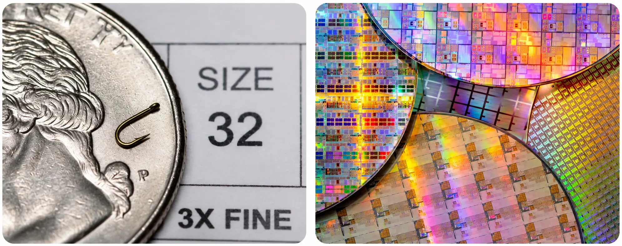
Summary: A tiny fishing hook and a 1,000-layer NAND flash memory chip have little in common at first glance. Yet both demonstrate how manufacturing complexity increases when engineers push established technologies toward their practical limits.
A fishing hook is about as simple a product as you can imagine. It’s a small piece of steel with a bend, a sharp point, and an eye for attaching fishing line. The basic design has been around for centuries, and there isn’t much about it that appears particularly complicated. That changes when you try manufacturing one in size #32.
For those unfamiliar with fly fishing, hook sizes generally become smaller as the number increases. A size #12 is fairly common, a #20 is small, and a #32 is exceptionally tiny. At that size, even threading fishing line through the eye can require magnification and a steady hand. But using the hook is only part of the challenge. Manufacturing something that small, while maintaining the strength and sharpness required to catch a fish, is surprisingly technical.
This got me thinking about Samsung’s work toward 1,000-layer NAND flash memory. The two products are obviously very different, but there is an interesting connection in the manufacturing processes, particularly when it comes to chemistry, precision, and the economics of making something at the extreme end of its design.
Making a Fishing Hook Isn’t Just Bending Wire
Manufacturing a fishing hook begins with selecting steel wire having the appropriate strength and flexibility. The wire is formed into the hook shape, heat-treated to achieve the desired mechanical properties, sharpened, and often coated to resist corrosion. These are well-established processes, but the tolerances become considerably more demanding as the hook gets smaller.
The wire must be thin enough for the desired hook size while retaining enough strength to function properly. The bend must be consistent, the eye must accommodate fishing line, and the point needs to be sharp without becoming excessively fragile. There isn’t much material available for correcting mistakes, which makes the manufacturing process more difficult than the finished product would suggest.
The Chemistry Behind a Sharp Hook
One of the more interesting aspects of fishing-hook manufacturing is how the point can be sharpened. Most people probably imagine a grinding wheel or abrasive surface removing metal until a sharp point is formed. While mechanical sharpeningA process of sharpening metal surfaces by physically grinding or abrading to create a sharp edge or point. is certainly used, some manufacturers also employ chemical polishing to refine the point.
In this process, a controlled chemical treatment dissolves small amounts of material from the metal surface, helping remove microscopic imperfections and produce a smooth, sharp point. The process is documented in Japanese fishing-hook manufacturing patents, including patent JP2015211649A, which describes chemical polishing during hook production and additional treatment of the point after surface finishing. An earlier Japanese patent also describes electrolytic polishing as a method of sharpening fishing hooks.
What makes this interesting is the amount of control required. Removing too little material may leave imperfections, while removing too much can compromise the point. Not every size #32 hook necessarily uses chemical sharpening, but the technology demonstrates how even a relatively simple metal product can depend on precise chemical processing.
And this is where the comparison with NAND flash memory becomes interesting.
From a Tiny Fishing Hook to 1,000 Layers of NAND
NAND flash memory has followed a similar progression of increasingly demanding manufacturing requirements, although on an entirely different scale. Early NAND chips arranged memory cells across the surface of a silicon wafer. As manufacturers approached the practical limits of shrinking those cells, the industry moved toward stacking memory cells vertically, creating what we now call 3D NAND.
Today, NAND manufacturers are producing increasingly complex vertical structures. Samsung introduced its V10 BV-NAND technology with more than 400 layers in 2026, while the broader semiconductor industry is working toward architectures containing 1,000 layers. The objective is to increase storage density without allowing manufacturing costs to grow faster than the additional capacity.
The challenge is that adding layers isn’t as simple as stacking another sheet of material onto a wafer. Manufacturers must deposit extremely thin films, maintain structural uniformity, and create microscopic vertical channels through the stack. As the number of layers increases, these channels become more difficult to manufacture with consistent dimensions from top to bottom.
One way to visualize the problem is to imagine drilling a very narrow hole through a tall stack of paper. Keeping the hole straight becomes more difficult as the stack gets taller. Semiconductor manufacturing is far more sophisticated, of course, but the basic challenge of maintaining a precise opening through an increasingly deep structure is similar.
Companies such as Lam Research are developing advanced plasma etching technologies to address these problems. Their work includes cryogenic etching, which uses low temperatures and specialized plasma chemistry to create deeper, more uniform structures within the NAND stack.
The Common Connection Is Controlled Material Removal
What I find particularly interesting is that both manufacturing processes can rely on chemistry to remove material with precision. A fishing-hook manufacturer may use chemical polishing to refine a steel point, while a semiconductor manufacturer uses plasma-based chemistry to etch microscopic features into a silicon wafer.
The processes are not directly comparable in complexity or precision. One deals with a small metal component, while the other involves microscopic structures manufactured using extraordinarily sophisticated equipment. However, both require careful control over how material is removed, how much is removed, and what remains after the process is complete.
For a fishing hook, an improperly finished point can affect its ability to penetrate and hold a fish. For NAND flash memory, an improperly etched channel can affect the electrical characteristics of memory cells or introduce defects that reduce manufacturing yield. The consequences are different, but both examples show why precision becomes increasingly important as manufacturing tolerances become tighter.
When Less Material Doesn’t Mean Lower Cost
There is also an economic connection worth considering. A size #32 fishing hook contains very little steel, yet that doesn’t necessarily make it inexpensive to manufacture. Specialized equipment, careful handling, additional inspection, and lower production yields can outweigh the savings in raw material. The manufacturer is paying for precision rather than the quantity of steel being used.
NAND manufacturers face a related problem. Increasing the number of memory layers can produce more storage capacity within a given wafer area, potentially reducing the cost per bit. However, additional layers also introduce more complicated processing requirements, expensive equipment, and greater opportunities for manufacturing defects. If those costs increase too quickly, the benefits of additional storage density begin to disappear.
This is why manufacturing yield matters so much. A company might demonstrate an impressive new technology in a laboratory, but commercial success requires producing it consistently and at an acceptable cost. Making one exceptionally small fishing hook or one exceptionally dense memory chip is not the same as manufacturing millions of them reliably.
Sometimes Simple Products Have Complicated Stories
We tend to associate advanced manufacturing with semiconductors, aircraft engines, medical equipment, and other products that appear technologically sophisticated. A fishing hook rarely comes to mind, even though its manufacturing process can involve carefully selected materials, controlled heat treatment, precise forming, and chemical surface finishing.
The same observation applies to the flash memory products we use every day. A microSD card is a small piece of plastic that can hold hundreds of gigabytes of information, yet its appearance gives almost no indication of the technology required to manufacture the memory inside.
There is no suggestion that manufacturing a size #32 fishing hook approaches the complexity of producing advanced NAND flash memory. The semiconductor industry operates at an entirely different level of precision, investment, and technical sophistication. What the two products share is the difficulty of pushing an established manufacturing process beyond what was previously practical.
Sometimes the most impressive engineering isn’t found in an entirely new invention. It’s found in the continued refinement of something we already know how to make, whether that’s a fishing hook small enough to be difficult to see or a NAND flash memory chip containing 1,000 layers.
References and Further Reading
- Japanese Patent JP2015211649A — Fishing-hook manufacturing process using chemical polishing and point finishing.
- Japanese Patent JPH04164525A — Electrolytic polishing method for sharpening fishing hooks.
- Lam Research: The Path to 1,000 Layers Will Be Etched — Technical discussion of advanced etching processes and NAND scaling.
- Samsung Semiconductor: V10 BV-NAND Beyond 400 Layers — Background on Samsung’s advanced NAND architecture.
- Counterpoint Research: Scaling to 1,000-Layer 3D NAND in the AI Era — Industry analysis of manufacturing challenges and future NAND scaling.
Technical Perspective: This article examines established fishing-hook manufacturing techniques and semiconductor fabrication technologies using publicly available patent documentation, semiconductor industry publications, and technical research. The comparison is intended to illustrate common manufacturing principles rather than suggest equivalent technical complexity. Specific manufacturing methods can vary by product and manufacturer.
Let GetUSB.info keep you updated.
Receive article notifications about USB storage, flash memory, and duplication updates in your preferred language. We average a couple of articles per week.