Samsung has publicly discussed building NAND flash memory with more than 1,000 layers by 2030. That sounds impressive, but what does it actually mean for the storage products we use? Will it be physically taller, harder to manufacture, less reliable, slower, or cheaper? And when will anyone be able to buy it?
Samsung’s 2022 roadmap identified more than 1,000 V-NAND layers as a goal for 2030. In August 2026, the company unveiled V10 Bonding V-NAND with more than 400 layers. Those are meaningful milestones, but the 1,000-layer target is not the same thing as a shipping product. Let’s work through eight practical questions, starting with the most basic one.
Eight Questions About Samsung’s 1,000-Layer NAND
- Are these really layers, like floors in a skyscraper?
- How physically tall will a 1,000-layer NAND chip be?
- How will engineers create the vertical channels?
- Can a 1,000-layer NAND chip actually be reliable?
- Will more layers make NAND slower to write?
- Will the controller need to be smarter and more powerful?
- Will fewer NAND chips make storage cheaper—or slower?
- Is Moore’s Law running out of steam, and when will 1,000-layer NAND arrive?
1. Are We Really Talking About 1,000 Layers, Like a 1,000-Story Building?
Yes. The building comparison is surprisingly accurate. Traditional planar NAND arranged memory cells across a flat surface. Three-dimensional NAND, also called V-NAND in Samsung’s terminology, builds additional cell layers upward. Think of the silicon footprint as a piece of land: rather than spreading out across a bigger lot, the manufacturer adds floors.
For perspective, the Burj Khalifa in Dubai, the world’s tallest completed building, has 163 above-ground floors and stands 828 meters (2,717 feet) tall. A 1,000-layer NAND array would have more than six times as many memory layers as the Burj Khalifa has floors. Of course, these floors are microscopic, not places people could walk around.
| Vertical structure | Floors or layers | What the number represents |
|---|---|---|
| Burj Khalifa | 163 | Building floors above ground |
| Samsung V10 (2026 unveiling) | 400+ | NAND memory layers |
| Samsung long-term goal | 1,000+ | Proposed NAND memory layers |
The analogy goes further. A skyscraper needs elevator shafts to connect floors. NAND needs vertical channel structures that pass through many memory-cell layers. The channels are part of the electrical architecture that makes the cells accessible, rather than simply empty holes or ordinary copper wires.
Bottom line: Samsung really does mean vertical memory layers. The challenge is making those microscopic floors and their electrical connections work consistently.
2. How Physically Tall Will 1,000-Layer NAND Be? Will the Finished Chip Be Bigger?
There are three different heights to consider: the height of the active memory array, the thickness of the silicon die, and the height of the finished packaged component soldered onto a circuit board. They are not interchangeable.
A taller memory array does not automatically require a taller final NAND package. Manufacturers can reduce the thickness of individual layers, thin the supporting silicon, change the way circuitry is arranged, and use advanced packaging methods.
Samsung has already shown that adding layers does not require a proportional increase in height. The company reported that its 176-layer seventh-generation V-NAND was similar in height to its earlier 100-plus-layer generation, in part because it reduced cell dimensions.
For a sense of scale, imagine an illustrative 45-nanometer vertical pitch per memory layer. Multiplying 1,000 layers by 45 nanometers gives 45 micrometers, or 0.045 millimeters, before adding extra structural and connection regions. That is roughly half the diameter of a typical human hair. This is a dimensional example, not Samsung’s announced 1,000-layer stack height or layer pitch.
The final package could remain similar in size to current NAND components, even if its internal architecture becomes more complex. That matters for USB flash drives, microSD cards, smartphones, and compact SSDs, where component height and circuit-board space are limited.
Bottom line: The internal stack will be more complex and may be taller, but a physically larger finished NAND package is not inevitable.
3. If the Vertical Channels Are So Deep, How Will Manufacturers Create Them?
This may be the most impressive manufacturing problem in the entire roadmap. Imagine creating a narrow hole through hundreds of microscopic material layers, keeping it aligned, maintaining its shape, and then lining its interior with precisely controlled materials. Now repeat that process millions or billions of times across a wafer.
The vertical channel is sometimes compared with a switchboard, but it is more accurately described as a shared electrical pathway through a string of memory cells. Word lines provide the control signals for cells at particular levels. The channel itself participates in the transistor structure; it is not merely a wire running past a series of separate switches.
Manufacturers do not use tiny mechanical drill bits. They use plasma-based semiconductor etching processes to remove material. As holes become deeper relative to their width, maintaining straight sidewalls, consistent dimensions, and acceptable etch rates becomes increasingly difficult. This is known as a high-aspect-ratio etching challenge.
New or substantially improved manufacturing equipment is part of the answer. Semiconductor equipment companies such as Lam Research and Tokyo Electron have invested in advanced high-aspect-ratio and cryogenic etching technologies. Cryogenic processes use carefully controlled low temperatures and plasma chemistry to improve etch behavior in difficult structures. Deposition equipment must also place thin films consistently along the channel walls after the holes are formed.
There is another important engineering option: do not attempt to etch all 1,000 layers in one uninterrupted operation. Multiple shorter stacks can be fabricated and connected, reducing the depth of any one etching step. Samsung’s V10 uses a three-stack approach, and its Bonding V-NAND architecture separately fabricates and bonds cell and peripheral circuitry wafers. These techniques help address different parts of the scaling problem; wafer bonding itself is not the same thing as joining every vertical channel.
But stacking sections introduces new alignment, interface, electrical resistance, and manufacturing-yield challenges. The problem does not disappear. It changes form.
Bottom line: Samsung cannot reach 1,000 layers by simply running today’s etching equipment longer. Equipment, materials, process control, and multi-stack integration must improve together.
4. If Making Those Channels Is Difficult, How Can 1,000-Layer NAND Be Reliable?
This question deserves skepticism. For years, buyers compared SLC, MLC, TLC, and later QLC NAND based on endurance, retention, and reliability. Each increase in bits stored per cell made it harder to distinguish the cell’s voltage states. A 1,000-layer structure seems to add another dimension of difficulty.
However, adding memory layers and storing more bits in each cell are two different engineering changes. SLC stores one bit per cell, MLC two, TLC three, and QLC four. Increasing bits per cell narrows the available voltage margins. Increasing the number of vertical layers instead adds fabrication, geometry, electrical uniformity, and integration challenges.
| Change | Main reliability challenge |
|---|---|
| SLC ? MLC ? TLC ? QLC | Smaller voltage margins, error sensitivity, endurance and retention trade-offs |
| 176 ? 400 ? 1,000 layers | Channel geometry, material uniformity, process defects, electrical behavior and yield |
Longer channels can be difficult to fabricate uniformly. A slight change in diameter from top to bottom, uneven film thickness, or variation in electrical resistance can change how individual cells behave. Some of those differences may make reads harder or reduce the margin for reliable programming.
Samsung’s V10 engineering discussion acknowledges challenges created by taller structures and describes improvements to channel profiles, process uniformity, and device operation. That is encouraging, but it is not the same as published long-term field reliability data for a future 1,000-layer product.
NAND controllers also help protect data. They use error-correction codes (ECC), bad-block management, wear leveling, and read-retry techniques. Manufacturers screen dies and characterize endurance and retention across operating conditions. Still, no amount of controller sophistication turns defective memory into perfect memory, and a chip passing factory tests is not a promise of indefinite unpowered data retention.
Does the difficulty rise exponentially? Not necessarily in a mathematical sense. More process steps and tighter tolerances can compound problems, but there is no justified formula saying that 1,000-layer NAND must be a particular percentage less reliable than 176-layer NAND.
Bottom line: The question is not whether Samsung can demonstrate a functioning 1,000-layer chip. It is whether it can manufacture large volumes that consistently meet endurance, retention, and error-rate requirements at an acceptable cost.
5. Will 1,000 Layers Make NAND Slower to Write?
Writing NAND is generally more demanding than reading it because programming changes the charge state of memory cells. More layers can introduce electrical complications, including longer channel paths and higher capacitive loads. But more layers do not automatically mean slower writes.
Three internal timing measurements matter: page program time (tPROG), page read time (tR), and block erase time (tBERS). These are different from the advertised megabytes-per-second throughput of an SSD or USB flash drive.
Samsung’s sixth-generation V-NAND, introduced in 2019, reported write-operation latency below 450 microseconds (0.450 milliseconds) and read latency below 45 microseconds (0.045 milliseconds), improving on the previous generation’s approximately 500 and 50 microseconds. In other words, Samsung increased layer count while reducing latency.
| Samsung generation | Write operation | Read operation |
|---|---|---|
| 5th-generation (9x layers) | ~0.500 ms | ~0.050 ms |
| 6th-generation (100+ layers) | <0.450 ms | <0.045 ms |
| Future 1,000-layer NAND | Unknown | Unknown |
To see why tiny changes matter, take 0.450 milliseconds as a hypothetical baseline. A 25% increase in program latency would produce 0.563 milliseconds; a 50% increase would produce 0.675 milliseconds; and a doubling would produce 0.900 milliseconds. These are illustrations, not forecasts for Samsung’s 1,000-layer NAND.
Bar lengths compare hypothetical latency against a 0.900 ms scale. No Samsung 1,000-layer latency has been announced.
There is also a more encouraging recent data point. Samsung says its V10 Bonding V-NAND achieves approximately 45% faster program performance and 33% faster NAND I/O than V9, despite exceeding 400 layers. Those improvements are Samsung-reported generation-to-generation figures; they do not mean every SSD built with V10 will write 45% faster.
At the device level, controllers write across multiple dies and planes, hide some operations through parallelism, and use caching. A storage product can therefore perform differently from its individual NAND dies. More density may help capacity but reduce the number of dies available for parallel writes at a given product capacity.
Bottom line: There is no sound way to multiply layer count into a future write-latency estimate. The challenge is whether architecture and circuitry improvements can offset the added electrical complexity.
6. Will 1,000-Layer NAND Need a Smarter, More Powerful Controller?
Possibly, but not simply because the controller has to remember which of 1,000 floors contain bad sectors. NAND generally manages physical pages and erase blocks, while a host computer sees logical sectors or logical block addresses. Bad-block information and mapping tables let the controller avoid unusable regions without scanning every block before each write.
Think of a hotel reservation system. It does not inspect every room whenever someone checks in. It already has records of which rooms are available, occupied, or out of service. A flash controller works with comparable bookkeeping, although its actual algorithms are far more complicated.
Greater NAND density may mean larger mapping structures, more physical blocks per die, or different scheduling requirements. But if two devices both provide 1 TB of capacity, a 1,000-layer version does not automatically require a proportionally larger mapping table than a 176-layer version. Mapping granularity, physical organization, firmware design, and available controller memory all matter.
| Controller task | Potential effect of denser NAND |
|---|---|
| Bad-block management | Track defective blocks and avoid allocating them |
| Wear leveling | Distribute erase cycles across usable blocks |
| Error correction | More processing or retries if raw errors increase |
| Flash translation layer | Maintain logical-to-physical mappings |
| Garbage collection | Move valid data before reclaiming blocks |
| Parallelism and scheduling | Balance work across available dies, planes and channels |
The more serious possible slowdown comes from error correction and data movement. If future NAND requires stronger ECC, more read-retry steps, or more garbage collection, the controller may spend additional time recovering or reorganizing data. Conversely, improvements in NAND quality and controller architecture can prevent those penalties.
Compare a 1 TB device made with older NAND to a 1 TB device made with much denser NAND: the logical capacity is unchanged, even if the number and organization of physical dies are different. Now compare a 1 TB device with an 8 TB device. The larger device has substantially more capacity to manage, but that is not proof that the number of vertical layers itself creates eight times the work.
Bottom line: Controllers will evolve, especially in error correction, scheduling and mapping. But more layers do not mean a linear increase in controller processing requirements.
7. Will Fewer NAND Chips Make Storage Cheaper—or Could That Make It Slower?
This is one of the strongest economic arguments for 1,000-layer NAND. If manufacturers can produce more usable bits per wafer, the cost per gigabyte may fall. A higher-capacity die could also allow an SSD or USB drive to reach its target capacity with fewer dies, potentially simplifying packaging and reducing component count.
But more layers do not automatically mean a proportionate increase in capacity. Die area, bits stored per cell, cell pitch, peripheral circuitry, spare area, and yield all affect usable density.
| Illustrative NAND design | Capacity per die | Dies for ~1 TB |
|---|---|---|
| Lower-density example | 512 Gb | 16 |
| Medium-density example | 1 Tb | 8 |
| Higher-density example | 2 Tb | 4 |
These are hypothetical die-capacity examples, not a Samsung product roadmap. For simplicity, 1 TB is treated as approximately 8 Tb before spare capacity and formatting overhead. A package can contain multiple NAND dies, so die count is not necessarily package count.
Now consider manufacturing economics. A future wafer might cost more to process because it requires additional etching, deposition, bonding, inspection, and testing. Yet if it produces much more usable storage, its cost per terabyte could still fall.
| Hypothetical manufacturing metric | Current process | Denser future process |
|---|---|---|
| Wafer processing cost | $5,000 | $8,000 |
| Usable storage per wafer | 100 TB | 250 TB |
| Wafer cost per usable TB | $50 | $32 |
In this illustration, wafer processing costs rise 60%, but cost per usable terabyte falls 36%. These figures are entirely hypothetical and exclude packaging, controllers, assembly, distribution and profit. They demonstrate the economics, not Samsung’s actual costs.
There is also a performance catch. SSD controllers achieve high throughput partly by writing to multiple NAND dies in parallel. Replacing 16 lower-capacity dies with four higher-capacity dies could reduce die-level parallelism. That may affect sustained writes, particularly after a drive exhausts its SLC cache. Faster interfaces, additional planes and better scheduling can help, but they may not eliminate the trade-off.
For a cost-sensitive USB flash drive, a manufacturer may prefer fewer dies and a lower bill of materials. For an enterprise SSD, maintaining consistent throughput may justify a different die configuration.
And even if NAND production costs decline, retail prices depend on supply, demand, capacity utilization, inventory and product positioning. Lower cost per bit does not guarantee an immediate reduction in the price customers pay.
Bottom line: The economic goal is not merely fewer chips. It is more usable, reliable storage per manufacturing dollar, without sacrificing too much performance.
8. Is Moore’s Law Running Out of Steam, and When Will Samsung Deliver 1,000-Layer NAND?
Gordon Moore, Intel’s co-founder, famously observed that transistor counts on integrated circuits tended to double on a roughly two-year cadence. The popular 18-month version is often associated with expectations about computing performance. Moore’s Law was an industry observation and economic expectation, not a physical law requiring progress to continue forever.
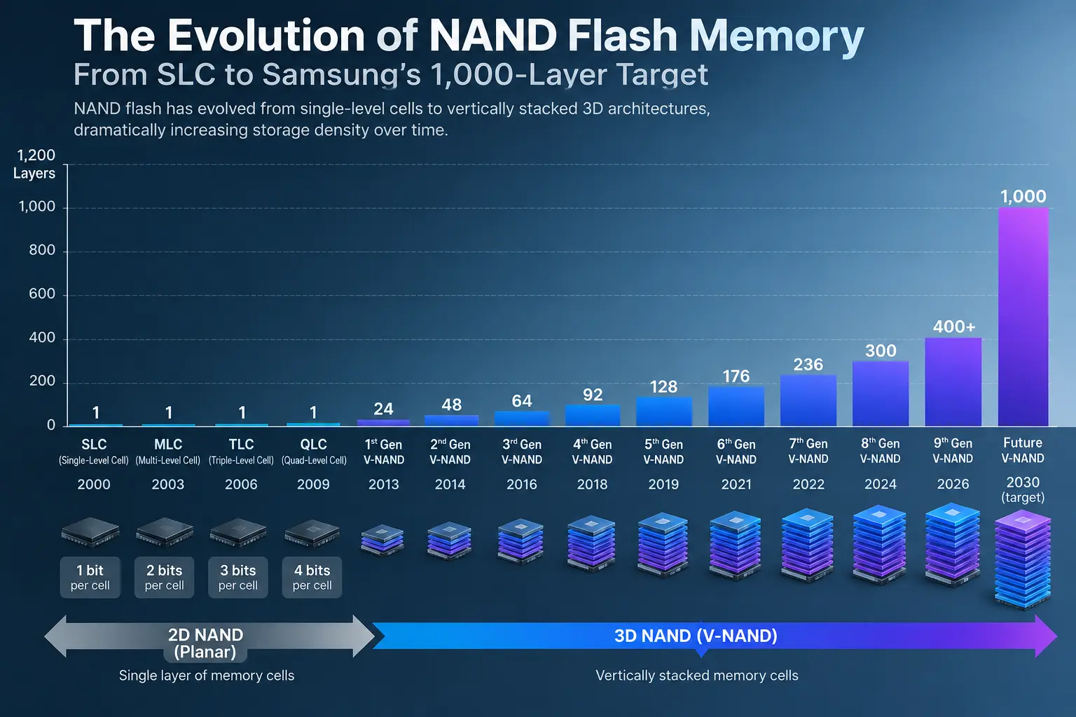
NAND manufacturers found another path to density: instead of only shrinking features across a flat chip, they built vertically. Samsung introduced its first commercial V-NAND in 2013 with 24 layers. Its 2026 V10 demonstration exceeds 400 layers. The company has publicly discussed going beyond 1,000 layers by 2030.
Bars show approximate layer counts on a 1,000-layer scale. The 2030 value is a target, not a shipping product.
The date is important, but so is the wording. At Samsung Tech Day 2022, the company said it envisioned stacking more than 1,000 layers by 2030. That is a development roadmap target, not a guaranteed mass-production or retail release date.
There are at least three milestones to separate: successfully demonstrating the technology, manufacturing it at economically acceptable yields, and shipping it inside finished SSDs, USB flash drives and other devices. Those milestones can occur at different times.
So is 1,000-layer NAND five years away or 25? Samsung’s publicly stated objective points to roughly 2030, only about four years from this article’s October 2026 publication date. But the exact timing of commercial availability remains unconfirmed.
Bottom line: Moore’s Law may no longer describe every step in semiconductor progress, but the drive for more bits per dollar continues. Whether 1,000-layer NAND becomes an affordable mainstream technology will depend as much on manufacturing economics and reliability as on reaching the headline layer count.
Final Thoughts: 1,000 Layers Is a Milestone, Not the Finish Line
Samsung’s plan is real. The company has publicly discussed exceeding 1,000 V-NAND layers by 2030, and its 400-plus-layer V10 announcement shows that development is progressing. But it is easy to confuse an impressive manufacturing milestone with an automatically better storage product.
For customers, the important questions remain familiar: How much storage do we get? How fast can we write it? How long will the data remain reliable? And what does it cost?
A 1,000-layer NAND chip that costs too much, suffers from poor manufacturing yields, or forces unacceptable performance compromises will not automatically win the market. The real achievement will be delivering greater density while preserving the reliability and economics that make flash memory useful in the first place.
That is why the road to 1,000 layers is worth following. Not because the number itself is magical, but because the engineering required to reach it will shape the next generation of SSDs, USB drives, memory cards, and other flash storage products.
Sources and Further Reading
- Samsung Tech Day 2022: 1,000+ V-NAND layers by 2030
- Samsung FMS 2026: V10 Bonding V-NAND with 400+ layers
- Samsung V10 engineering and development discussion
- Samsung: The Story Behind V-NAND
- Samsung: Sixth-generation V-NAND latency and channel-hole technology
- The Skyscraper Center: Burj Khalifa building data
Let GetUSB.info keep you updated.
Receive article notifications about USB storage, flash memory, and duplication updates in your preferred language. We average a couple of articles per week.