AI systems don’t typically slow down because of compute limitations, but rather because the system cannot move data fast enough to keep the processor consistently fed with information.
In other words, the bottleneck is not the ability to process data, but the ability to deliver that data at the speed modern AI workloads require.
This is where High Bandwidth Memory (HBM) becomes an important part of the architecture.
For a broader look at how memory is evolving beyond flash and why AI systems now depend on multiple tiers, see our main analysis: NAND isn’t going away, but AI servers now depend on more than flash.
What is High Bandwidth Memory (HBM)?
High Bandwidth Memory is a type of stacked DRAM that is placed extremely close to the processor, often just millimeters away from the GPU die, in order to minimize the physical distance data must travel.
Unlike traditional system memory, which relies on longer electrical pathways and narrower data channels, HBM is designed around proximity and parallelism, allowing significantly more data to move at once and with far less delay.
- Wide memory buses, often thousands of bits wide
- Ultra-short trace distances between memory and processor
- Massively parallel access to data
The goal is straightforward: reduce the distance between where data is stored and where it is processed, because in high-performance systems, even small delays add up quickly.
In practical terms, distance translates directly into latency, and latency is one of the primary factors limiting AI performance.
A Simple Way to Think About HBM
A helpful way to visualize this is to think of a traditional system as a factory connected to a warehouse by a highway.
Every time the factory needs parts, those parts must be transported back and forth, which introduces delays, increases energy use, and limits how quickly the system can operate.
HBM changes that relationship by effectively stacking the warehouse directly on top of the factory floor.
Instead of relying on transportation, everything is immediately accessible, which eliminates the delays associated with moving data across longer distances.
This is essentially what HBM does for a GPU, placing memory so close to the compute engine that data movement becomes almost instantaneous compared to traditional designs.
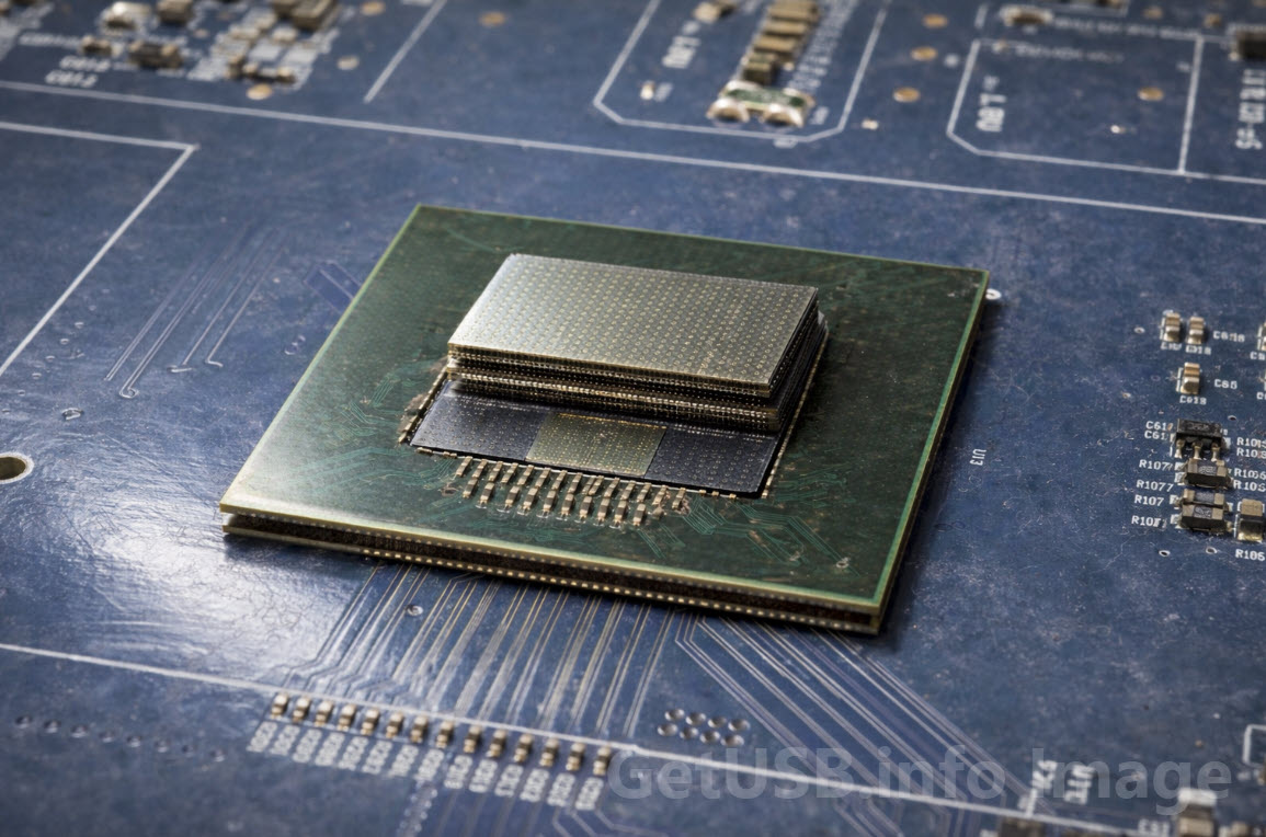
How HBM is Physically Built
The advantage of HBM is not just in layout, but in how the memory itself is constructed at the silicon level.
HBM is built by stacking multiple DRAM dies vertically and connecting them using Through-Silicon Vias (TSVs), which are microscopic vertical pathways drilled through the silicon to allow direct electrical connections between layers.
These stacked memory modules are then mounted on an interposer alongside the GPU, forming a tightly integrated package where memory and compute operate as a unified system rather than separate components.
The result is a combination of extremely wide data paths and very short electrical distances, which together enable the high bandwidth that defines HBM.
Why AI Depends on HBM
AI workloads, particularly training models, require continuous movement of large amounts of data, often involving billions or even trillions of parameters that must be read, updated, and rewritten repeatedly.
This creates a demand for both high bandwidth, to move large datasets quickly, and low latency, to ensure the compute engines are not left idle waiting for data.
- High bandwidth ensures large volumes of data can be transferred quickly
- Low latency ensures compute units remain fully utilized
Traditional memory architectures struggle to meet both of these requirements at the same time, which is why HBM has become a standard component in high-end AI accelerators.
Without HBM, even the most powerful GPU would spend a significant portion of its time waiting for data instead of processing it.
The Trade-Off: Speed vs Cost
While HBM provides significant performance advantages, it also introduces additional complexity and cost due to its stacked design and advanced packaging requirements.
The use of multiple DRAM layers, precision interconnects, and interposer-based integration makes HBM one of the more expensive memory technologies currently available.
Because of this, it is typically reserved for applications where performance is critical and the cost can be justified, such as AI training and high-performance computing environments.
General-purpose systems, where cost sensitivity is higher, continue to rely on more conventional memory solutions.
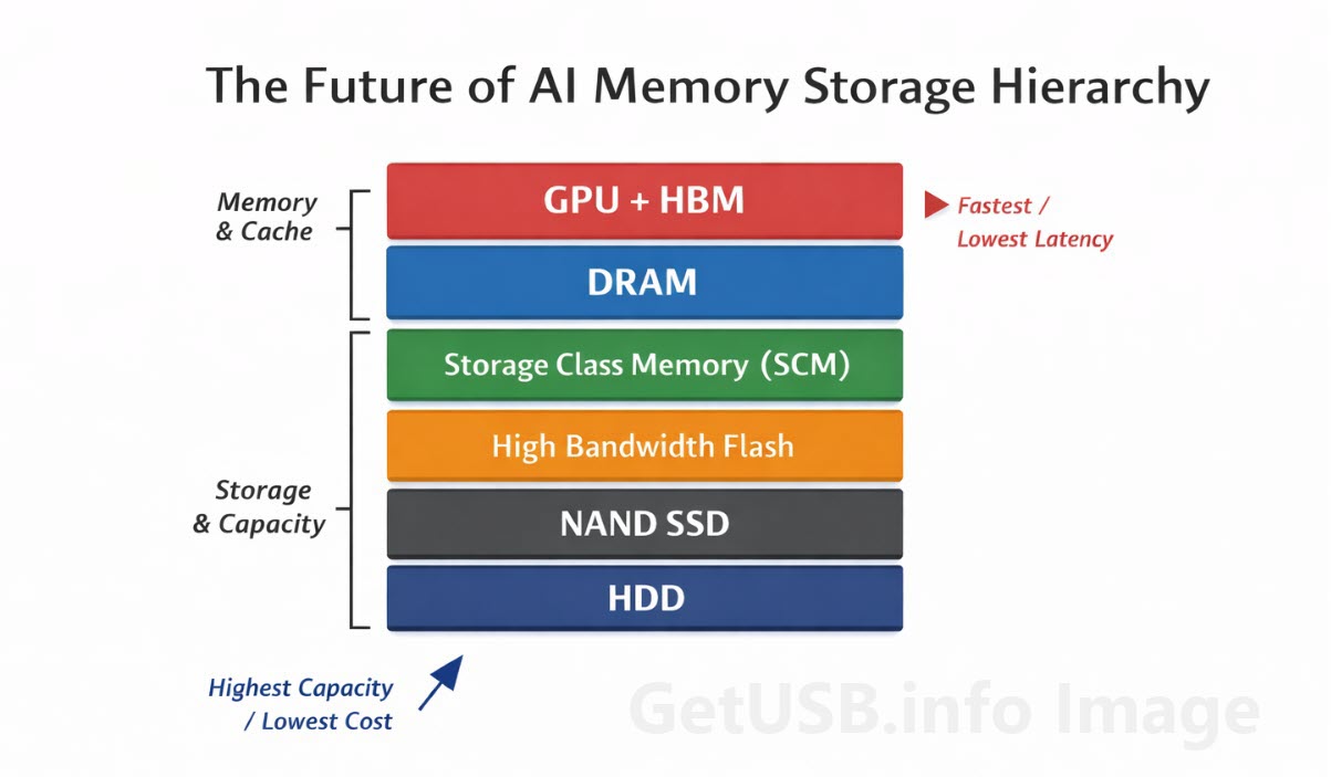
Where HBM Fits in the Bigger Picture
HBM does not replace other types of memory, but instead sits at the top of a layered memory hierarchy, where each layer is optimized for a different balance of speed, cost, and capacity.
| Technology | Typical Latency | Bandwidth | Cost per GB | Primary Role |
|---|---|---|---|---|
| HBM (Stacked DRAM) | Nanoseconds | Terabytes/sec | Very High | AI training memory |
| DDR DRAM | ~100ns | High | High | System memory |
| NVMe SSD | Microseconds–Milliseconds | Moderate | Low | Bulk storage |
Each layer exists because of trade-offs between performance, cost, and capacity, and no single technology can optimize all three at once.
HBM occupies the highest-performance tier, where speed is prioritized over cost, making it essential for workloads that cannot tolerate delays.
The Shift
HBM should not be thought of as simply faster memory, but rather as a shift in system design that brings memory physically closer to compute in order to remove one of the biggest bottlenecks in modern computing.
In AI systems, where performance is directly tied to how quickly data can be accessed and processed, this architectural change plays a critical role.
Ultimately, even the most advanced processors depend on a steady flow of data, and improving that flow is what makes technologies like HBM so important.
Editorial and image note: This article was directed and reviewed by GetUSB.info based on our editorial research and technical understanding of memory packaging and storage hardware.
Image disclosure: The image used with this article is based on a real-world chip photograph and was enhanced to better illustrate the HBM concept for readers. The enhancement was done for visual explanation only, so the image should be understood as a realistic interpretive graphic rather than a literal manufacturing reference photo.
How this article was created: GetUSB.info provided the topic direction, technical angle, and final editorial review. AI tools were used to assist with rhythm and flow, with human oversight applied throughout the process.