Have you ever been taking a shower when someone turns on the washing machine and suddenly your water pressure drops? There is nothing wrong with your shower, and there is nothing wrong with your washing machine. The problem is the plumbing infrastructure supporting both of them.
A well-designed plumbing system can deliver water to multiple locations without one appliance interfering with another. The appliances are exactly the same; they simply have better infrastructure supporting them.
Believe it or not, the same philosophy applies to the construction of a USB flash drive.
When shopping for a USB flash drive, most people look at storage capacity, read and write speeds, and whether the device supports USB 2.0 or USB 3.0. Those who know a little more about flash memory might inquire about the NAND manufacturer or the type of controller being used.
But when was the last time someone asked how many layers were in the printed circuit board?
Probably never. Yet it’s a manufacturing decision worth understanding, particularly for businesses that depend on flash memory for commercial applications.
What Is a 4-Layer PCB?
The printed circuit board, or PCB, is the small board inside a USB flash drive that connects all the electronic components. The USB controller, NAND flash memory, capacitors, resistors and other components all depend on this board to communicate and receive power.
A two-layer PCB has copper circuitry on the top and bottom of the board. All the electrical connections, power distribution and grounding must be accommodated within those two layers. It’s a perfectly legitimate way to manufacture a USB flash drive and a common approach in the commodity flash drive market.
A four-layer PCB takes a different approach. Between the top and bottom layers are two additional layers of copper, separated by insulating material. A well-designed four-layer USB flash drive can use the following configuration:
- Layer 1 – Signal traces and components
- Layer 2 – Dedicated ground plane
- Layer 3 – Dedicated power plane
- Layer 4 – Signal traces and components
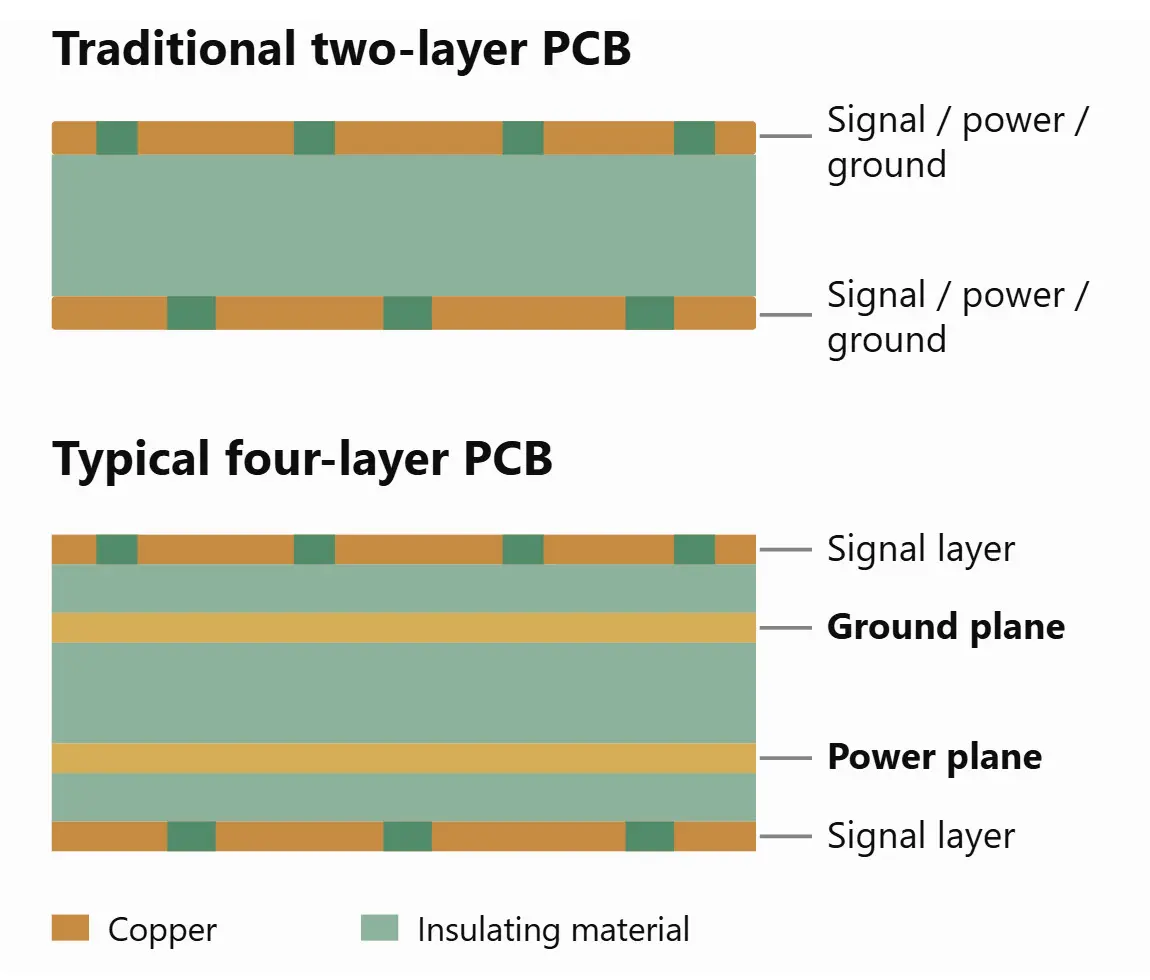
What’s particularly interesting is that the two additional layers aren’t necessarily there to accommodate more components or more sophisticated features. They are there to improve the electrical environment in which the existing components operate.
Why a Dedicated Ground Plane Matters
Every electrical signal requires a return path. When the USB controller sends information to the NAND flash memory, there is also an electrical current that needs to find its way back.
On a two-layer PCB, the engineer must work around other electrical connections and components to establish that return path. Depending on the layout, the return current may need to take a less direct route.
On a four-layer PCB, an entire layer of copper can be dedicated to ground. This allows high-frequency return currents to travel directly beneath their corresponding signal traces when routed adjacent to the ground plane, providing a more direct and predictable electrical path.
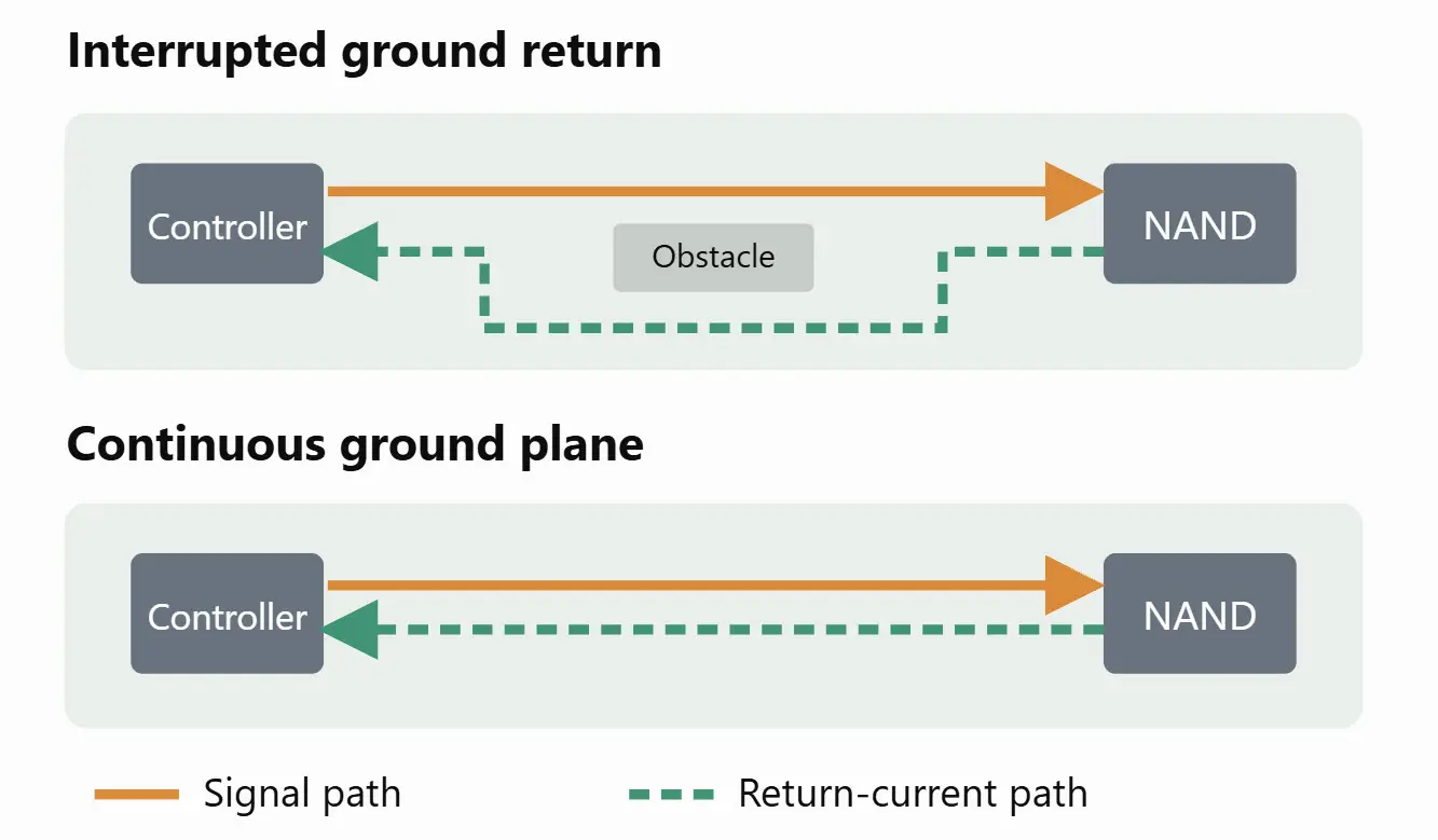
Why does this matter? Because the larger the loop created by a signal and its return path, the greater the opportunity for electromagnetic interference. A continuous ground plane helps minimize that loop.
It also helps reduce something called crosstalk, which is essentially one electrical signal interfering with another nearby signal. Considering how small the circuit board inside a USB flash drive is, and how many electrical connections are packed into that space, it’s easy to appreciate the benefit.
The result is an environment with less electrical noise and better signal integrity. In simple terms, the electronic components have a better opportunity to communicate clearly with one another.
A Dedicated Power Plane Is Equally Interesting
Getting back to our plumbing example, imagine the USB controller is the washing machine and the NAND flash memory is the shower. Both need a consistent supply of power, but their demands can change depending on what they’re doing.
Reading data, writing data and erasing flash memory are different electrical operations. The amount of current required by the components can fluctuate as the USB flash drive performs these tasks.
On a two-layer PCB, power is distributed using copper traces and larger areas of copper wherever space permits. On a four-layer board, a dedicated power plane provides a much larger area through which power can be distributed.
When combined with properly positioned capacitors, this helps manage fluctuations in electrical demand and maintain a more stable voltage supply to the components.
It’s particularly beneficial during sustained write operations, when a USB flash drive is actively programming large amounts of data into the NAND memory.
Anyone who has experienced an intermittent problem with an electronic device knows how frustrating those problems can be to identify. The device works fine nine times out of ten, but that tenth time creates a problem that is difficult to reproduce. Maintaining stable power delivery is one of the ways engineers can reduce the potential for electrically induced problems.
Comparing a 2-Layer PCB to a 4-Layer PCB
Here is a general comparison of the two manufacturing approaches.
| Characteristic | Typical 2-layer PCB | Well-designed 4-layer PCB |
|---|---|---|
| Ground reference | Shared or potentially interrupted | Dedicated, continuous ground plane |
| Electrical noise | More difficult to manage | Easier to manage |
| Power distribution | Primarily traces and copper pours | Dedicated power plane |
| Signal integrity | More design constraints | Greater control |
| EMI suppression | More challenging | Improved potential |
| Manufacturing cost | Lower | Higher |
| NAND endurance | Unchanged | Unchanged |
| Electrical reliability | Design dependent | Greater potential design margin |
It’s worth pointing out that a four-layer PCB does not increase the number of times a NAND memory cell can be written to or erased. That is a characteristic of the NAND memory itself, something we’ve discussed previously in our article about MLC versus TLC NAND flash memory. Nor does four-layer construction automatically make a USB flash drive faster.
What it does provide is a better electrical infrastructure for those components.
Does a USB 2.0 Flash Drive Really Need Four Layers?
This is a fair question. After all, USB 2.0 technology has been around for over two decades, and countless USB 2.0 devices have been manufactured using two-layer circuit boards.
However, USB 2.0 High-Speed operates at 480 megabits per second. While that might not sound particularly impressive compared to today’s USB 3.0 technology, it is still a high-frequency electrical interface that requires attention to signal integrity.
There is also another factor to consider. The advertised speed of a USB flash drive describes its external interface, but there is an entirely separate communication interface between the USB controller and the NAND flash memory. Those internal signals have their own electrical requirements.
Even a device with a relatively modest data transfer rate can have rapidly changing electrical signals that benefit from a continuous ground plane.
The argument for using four layers in a USB 2.0 device isn’t necessarily about speed. It’s about something electrical engineers refer to as design margin.
What Is Electrical Design Margin?
Let’s say you’re building a shelf that needs to support 100 pounds. You could build a shelf rated for exactly 100 pounds, or you could build one rated for 150 pounds. Both shelves meet your original requirement, but one gives you a little more room for unexpected circumstances.
That’s essentially the idea behind engineering design margin.
Not every computer delivers power to its USB ports under identical conditions. Electronic components have manufacturing tolerances. Operating temperatures vary. Electrical interference can differ from one operating environment to another.
These are normal circumstances, not necessarily faults or defects.
A USB flash drive with greater electrical design margin is better positioned to accommodate these variations without compromising its operation, assuming the rest of the device is properly engineered.
For a consumer transferring a few photographs, these considerations might not be particularly interesting. For a company deploying 50,000 USB flash drives into the field, it’s an entirely different conversation.
That company isn’t necessarily looking for the fastest flash drive. It’s looking for the most predictable flash drive.
Why Don’t All Manufacturers Use 4-Layer PCBs?
As with many things in manufacturing, it comes down to money.
A four-layer printed circuit board requires additional copper layers, insulating material, processing, lamination and manufacturing precision. There are more steps involved in producing the board, so naturally it costs more.
But how much more?
For a small circuit board, such as one found inside a typical USB flash drive, an illustrative estimate for high-volume manufacturing might look something like this:
| PCB Construction | Estimated Cost Per Board |
|---|---|
| 2-layer PCB | $0.08–$0.12 |
| 4-layer PCB | $0.16–$0.24 |
| Additional cost | Approximately $0.10 |
These figures are illustrative estimates for the bare circuit board, not actual factory quotations. Pricing will vary depending on production volume, board dimensions and manufacturing specifications.
A manufacturer could potentially double the cost of the printed circuit board, yet the additional expense per USB flash drive might only be around ten cents.
Of course, if you’re manufacturing one million USB flash drives, ten cents represents $100,000 in additional manufacturing costs. For a manufacturer competing primarily on price, it’s easy to understand the motivation to use a two-layer design.
From the perspective of a business purchasing USB flash drives for a commercial application, however, that same ten cents looks considerably different.
Consider the time and expense associated with investigating a product failure, replacing a device in the field or troubleshooting an intermittent problem reported by a customer. The additional investment in PCB construction is relatively small compared to the potential cost of dealing with an unreliable product.
Why PCB Construction Matters for Commercial Applications
USB flash drives are used for considerably more than personal file storage. Pharmaceutical companies distribute product information and documentation on USB media. Medical equipment manufacturers use flash drives for software distribution, configuration files and equipment updates. Industrial companies use them for data collection and the operation of embedded systems.
In many of these applications, the USB flash drive is just one small component of a much larger business operation. Nobody wants that little device to become the reason something else doesn’t work.
Consistency is particularly important when purchasing flash memory in large volumes. A device that performs well during an initial qualification process needs to continue performing predictably throughout subsequent production runs.
Using a four-layer PCB gives engineers additional flexibility to design for normal variations in components, manufacturing tolerances and operating conditions.
Of course, PCB construction is only one consideration when qualifying a USB flash drive for commercial use. NAND quality, controller firmware, component selection, manufacturing controls and product testing are all important. A four-layer board is not a substitute for any of them, just as a properly designed two-layer board is not inherently unreliable.
Based on Our Years of Experience
After nearly two decades of covering USB technology and working with flash memory products, we’ve come to appreciate the manufacturing decisions that don’t typically make it onto a product specification sheet. As we’ve discussed before, speed is easy, reliability is hard, and that philosophy applies just as much to the construction of a storage device as it does to the way data is transferred.
The next time you’re evaluating USB flash drives for a commercial application, consider asking the manufacturer how many layers are used in the printed circuit board. If the answer is four, ask how those layers are utilized.
It’s a relatively simple question that can reveal something about the engineering philosophy behind the product.
We tend to evaluate technology based on the things we can measure easily. Storage capacity, transfer speed and price are all readily available numbers. Electrical stability and design margin are considerably more difficult to quantify from a product specification sheet.
Yet for businesses that prioritize reliability, stability and consistency, those less visible manufacturing decisions may be among the most important.
Sometimes the quality of a product isn’t just about the components a manufacturer puts into it. It’s also about how well those components are supported.
About this article: GetUSB.info has been covering USB technology, flash memory, storage devices and data duplication since 2006. This article draws upon hands-on industry experience with USB flash drive construction, component selection, manufacturing and commercial deployment. The technical discussion is based on established PCB design principles, with manufacturing costs provided as illustrative estimates rather than specific supplier quotations.
Let GetUSB.info keep you updated.
Receive article notifications about USB storage, flash memory, and duplication updates in your preferred language. We average a couple of articles per week.